- 定價200.00元
-
8
折優惠:HK$160

|
|
|
|
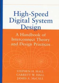
HIGH-SPEED DIGITAL SYSTEM DESIGN: A HANDBOOK OF INTERCONNECT THEORY AND DESIGN
|

|

沒有庫存
訂購需時10-14天
|
|
|
|

|
|
9780471360902 | |
|

|
|
HALL | |
|

|
|
全華圖書 | |
|

|
|
2000年1月01日
| |
|

|
|
433.00 元
| |
|

|
|
HK$ 411.35
|
|
|
|
|

| |
|
|
|
|
| |
|
|
詳
細
資
料
|
叢書系列:實用電子
規格:精裝 / 348頁 / 普級 / 單色印刷 / 初版
出版地:台灣
實用電子
|
|
分
類
|
專業/教科書/政府出版品 > 電機資訊類 > 電子 |
同
類
書
推
薦
|
|
|
內
容
簡
介
|
An understanding of high-speed interconnect phenomena is essential for digital designers who must deal with the challenges posed by the ever-increasing operating speeds of today’s microprocessors. This book provides a much-needed, practical guide to the state of the art of modern digital system design, combining easily accessible explanations with immensely useful problem-solving strategies. Written by three leading Intel engineers, High-Speed Digital System Design clarifies difficult and often neglected topics involving the effects of high frequencies on digital buses and presents a variety of proven techniques and application examples. Extensive appendices, formulas, modeling techniques as well as hundreds of figures are also provided.
|
|
目
錄
|
Preface.
1. The Importance of Interconnect Design.
1.1 The Basics.
1.2 The Past and the Future.
2. Ideal Transmission Line Fundamentals.
2.1 Transmission Line Structures on a PCB or MCM.
2.2 Wave Propagation.
2.3 Transmission Line Parameters.
2.3.1 Characteristic Impedance.
2.3.2 Propagation Velocity, Time, and Distance.
2.3.3 Equivalent Circuit Models for SPICE Simulation.
2.4 Launching Initial Wave and Transmission Line Reflections.
2.4.1 Initial Wave.
2.4.2 Multiple Reflections.
2.4.3 Effect of Rise Time on Reflections.
2.4.4 Reflections From Reactive Loads.
2.4.5 Termination Schemes to Eliminate Reflections.
2.5 Additional Examples.
2.5.1 Problem.
2.5.2 Goals.
2.5.3 Calculating the Cross-Sectional Geometry of the PCB.
2.5.4 Calculating the Propagation Delay.
2.5.5 Determining the Wave Shape Seen at the Receiver.
2.5.6 Creating an Equivalent Circuit.
3. Crosstalk.
3.1 Mutual Inductance and Mutual Capacitance.
3.2 Inductance and Capacitance Matrix.
3.3 Field Simulators.
3.4 Crosstalk-Induced Noise.
3.5 Simulating Crosstalk Using Equivalent Circuit Models.
3.6 Crosstalk-Induced Flight Time and Signal Integrity Variations.
3.6.1 Effect of Switching Patterns on Transmission Line Performance.
3.6.2 Simulating Traces in a Multiconductor System Using a Single-Line Equivalent Model.
3.7 Crosstalk Trends.
3.8 Termination of Odd- and Even-Mode Transmission Line Pairs.
3.8.1 Pi Termination Network.
3.8.2 T Termination Network.
3.9 Minimization of Crosstalk.
3.10 Additional Examples.
3.10.1 Problem.
3.10.2 Goals.
3.10.3 Determining the Maximum Crosstalk-Induced Impedance and Velocity Swing.
3.10.4 Determining if Crosstalk Will Induce False Triggers.
4. Nonideal Interconnect Issues.
4.1 Transmission Line Losses.
4.1.1 Conductor DC Losses.
4.1.2 Dielectric DC Losses.
4.1.3 Skin Effect.
4.1.4 Frequency-Dependent Dielectric Losses.
4.2 Variations in the Dielectric Constant.
4.3 Serpentine Traces.
4.4 Intersymbol Interference.
4.5 Effects of 90 Bends.
4.6 Effect of Topology.
5. Connectors, Packages, and Vias.
5.1 Vias.
5.2 Connectors.
5.2.1 Series Inductance.
5.2.2 Shunt Capacitance.
5.2.3 Connector Crosstalk.
5.2.4 Effects of Inductively Coupled Connector Pin Fields.
5.2.5 EMI.
5.2.6 Connector Design Guidelines.
5.3 Chip Packages.
5.3.1 Common Types of Packages.
5.3.2 Creating a Package Model.
5.3.3 Effects of a Package.
5.3.4 Optimal Pin-Outs.
6. Nonideal Return Paths, Simultaneous Switching Noise, and Power Delivery.
6.1 Nonideal Current Return Paths.
6.1.1 Path of Least Inductance.
6.1.2 Signals Traversing a Ground Gap.
6.1.3 Signals That Change Reference Planes.
6.1.4 Signals Referenced to a Power or a Ground Plane.
6.1.5 Other Nonideal Return Path Scenarios.
6.1.6 Differential Signals.
6.2 Local Power Delivery Networks.
6.2.1 Determining the Local Decoupling Requirements for High-Speed I/O.
6.2.2 System-Level Power Delivery.
6.2.3 Choosing a Decoupling Capacitor.
6.2.4 Frequency Response of a Power Delivery System.
6.3 SSO/SSN.
6.3.1 Minimizing SSN.
7. Buffer Modeling.
7.1 Types of Models.
7.2 Basic CMOS Output Buffer.
7.2.1 Basic Operation.
7.2.2 Linear Modeling of the CMOS Buffer.
7.2.3 Behavioral Modeling of the Basic CMOS Buffer.
7.3 Output Buffers That Operate in the Saturation Region.
7.4 Conclusions.
8. Digital Timing Analysis.
8.1 Common-Clock Timing.
8.1.1 Common-Clock Timing Equations.
8.2 Source Synchronous Timing.
8.2.1 Source Synchronous Timing Equations.
8.2.2 Deriving Source Synchronous Timing Equations from an Eye Diagram.
8.2.3 Alternative Source Synchronous Schemes.
8.3 Alternative Bus Signaling Techniques.
8.3.1 Incident Clocking.
8.3.2 Embedded Clock.
9. Design Methodologies.
9.1 Timings.
9.1.1 Worst-Case Timing Spreadsheet.
9.1.2 Statistical Spreadsheets.
9.2 Timing Metrics, Signal Quality Metrics, and Test Loads.
9.2.1 Voltage Reference Uncertainty.
9.2.2 Simulation Reference Loads.
9.2.3 Flight Time.
9.2.4 Flight-Time Skew.
9.2.5 Signal Integrity.
9.3 Design Optimization.
9.3.1 Paper Analysis.
9.3.2 Routing Study.
9.4 Sensitivity Analysis.
9.4.1 Initial Trend and Significance Analysis.
9.4.2 Ordered Parameter Sweeps.
9.4.3 Phase 1 Solution Space.
9.4.4 Phase 2 Solution Space.
9.4.5 Phase 3 Solution Space.
9.5 Design Guidelines.
9.6 Extraction.
9.7 General Rules of Thumb to Follow When Designing a System.
10. Radiated Emissions Compliance and System Noise Minimization.
10.1 FCC Radiated Emission Specifications.
10.2 Physical Mechanisms of Radiation.
10.2.1 Differential-Mode Radiation.
10.2.2 Common-Mode Radiation.
10.2.3 Wave Impedance.
10.3 Decoupling and Choking.
10.3.1 High-Frequency Decoupling at the System Level.
10.3.2 Choking Cables and Localized Power and Ground Planes.
10.3.3 Low-Frequency Decoupling and Ground Isolation.
10.4 Additional PCB Design Criteria, Package Considerations, and Pin-Outs.
10.4.1 Placement of High-Speed Components and Traces.
10.4.2 Crosstalk.
10.4.3 Pin Assignments and Package Choice.
10.5 Enclosure (Chassis) Considerations.
10.5.1 Shielding Basics.
10.5.2 Apertures.
10.5.3 Resonances.
10.6 Spread Spectrum Clocking.
11. High-Speed Measurement Techniques.
11.1 Digital Oscilloscopes.
11.1.1 Bandwidth.
11.1.2 Sampling.
11.1.3 Other Effects.
11.1.4 Statistics.
11.2 Time-Domain Reflectometry.
11.2.1 TDR Theory.
11.2.2 Measurement Factors.
11.3 TDR Accuracy.
11.3.1 Launch Parasitics.
11.3.2 Probe Types.
11.3.3 Reflections.
11.3.4 Interface Transmission Loss.
11.3.5 Cable Loss.
11.3.6 Amplitude Offset Error.
11.4 Impedance Measurement.
11.4.1 Accurate Characterization of Impedance.
11.4.2 Measurement Region in TDR Impedance Profile.
11.5 Odd- and Even-Mode Impedance.
11.6 Crosstalk Noise.
11.7 Propagation Velocity.
11.7.1 Length Difference Method.
11.7.2 Y-Intercept Method.
11.7.3 TDT Method.
11.8 Vector Network Analyzer.
11.8.1 Introduction to S Parameters.
11.8.2 Equipment.
11.8.3 One-Port Measurements (ZO,L,C).
11.8.4 Two-Port Measurements (Td, Attenuation, Crosstalk).
11.8.5 Calibration.
11.8.6 Calibration for One-Port Measurements.
11.8.7 Calibration for Two-Port Measurements.
11.8.8 Calibration Verification.
Appendix A: Alternative Characteristic Impedance Formulas.
A.1 Microstrip.
A.2 Symmetric Stripline.
A.3 Offset Stripline.
Appendix B: GTL Current-Mode Analysis.
B.1 Basic GTL Operation.
B.2 GTL Transitions When a Middle Agent Is Driving.
B.3 GTL Transitions When an End Agent With a Termination Is Driving.
B.4 Transitions When There is a Pull-Up at the Middle Agent.
Appendix C: Frequency-Domain Components in a Digital Signal.
Appendix D: Useful S-Parameter Conversions.
D.1 ABCD, Z, and Y Parameters.
D.2 Normalizing the S Matrix to a Different Characteristic Impedance.
D.3 Derivation of the Formulas Used to Extract the Mutual Inductance and Capacitance from a Short Structure Using S21 Measurements.
D.4 Derivation of the Formula to Extract Skin Effect Resistance from a Transmission Line.
Appendix E: Definition of the Decibel.
Appendix F: FCC Emission Limits.
Bibliography.
Index.
|
|
|
書
評
|
|
|
|
|

